Trending...
- DriveYo Signs Cybersecurity Prodigy and Open-Source Pioneer Utkarsh Lubal - 101
- Alchemy 43 Appoints Shane Smith as CEO to Drive Operational Performance and Scalable Growth
- Ashikaga Flower Park's "Great Wisteria Festival 2026"
Download
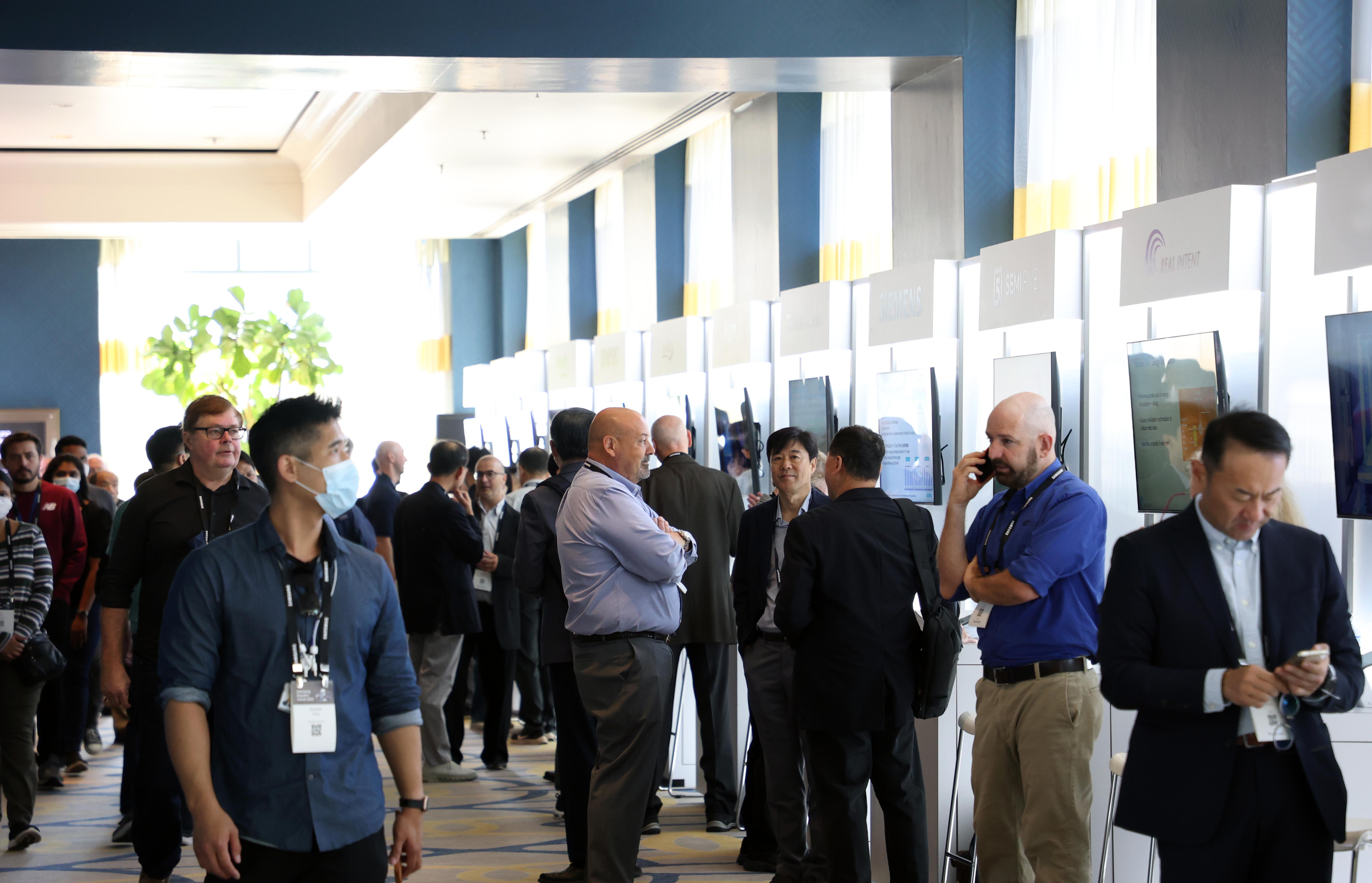
Attendees of Samsung Foundry Forum 2022 are gathered around the customer booths. (Photo: Business Wire)
SAN JOSE, Calif.--(BUSINESS WIRE)--Samsung Electronics, a world leader in advanced semiconductor technology, announced today a strengthened business strategy for its Foundry Business with the introduction of cutting-edge technologies at its annual Samsung Foundry Forum event.
More on The Californer
With significant market growth in high-performance computing (HPC), artificial intelligence (AI), 5/6G connectivity and automotive applications, demand for advanced semiconductors has increased dramatically, making innovation in semiconductor process technology critical to the business success of foundry customers. To that end, Samsung highlighted its commitment to bringing its most advanced process technology, 1.4-nanometer (nm), for mass production in 2027.
During the event, Samsung also outlined steps its Foundry Business is taking in order to meet customers' needs, including: foundry process technology innovation, process technology optimization for each specific applications, stable production capabilities, and customized services for customers.
"The technology development goal down to 1.4nm and foundry platforms specialized for each application, together with stable supply through consistent investment are all part of Samsung's strategies to secure customers' trust and support their success," said Dr. Si-young Choi, president and head of Foundry Business at Samsung Electronics. "Realizing every customer's innovations with our partners has been at the core of our foundry service."
Showcasing Samsung's Advanced Node Roadmap Down to 1.4nm in 2027
With the company's success of bringing the latest 3nm process technology to mass production, Samsung will be further enhancing gate-all-around (GAA) based technology and plans to introduce the 2nm process in 2025 and 1.4nm process in 2027.
While pioneering process technologies, Samsung is also accelerating the development of 2.5D/3D heterogeneous integration packaging technology to provide a total system solution in foundry services.
Through continuous innovation, its 3D packaging X-Cube with micro-bump interconnection will be ready for mass production in 2024, and bump-less X-Cube will be available in 2026.
Proportion of HPC, Automotive and 5G to be More than 50% by 2027
Samsung actively plans to target high-performance and low-power semiconductor markets such as HPC, automotive, 5G and the Internet of Things (IoT).
To better meet customers' needs, customized and tailored process nodes were introduced during this year's Foundry Forum. Samsung will enhance its GAA-based 3nm process support for HPC and mobile, while further diversifying the 4nm process specialized for HPC and automotive applications.
For automotive customers specifically, Samsung is currently providing embedded non-volatile memory (eNVM) solutions based on 28nm technology. In order to support automotive-grade reliability, the company plans to further expand process nodes by launching 14nm eNVM solutions in 2024 and adding 8nm eNVM in the future. Samsung has been mass producing 8nm RF following 14nm RF, and 5nm RF is currently in development.
'Shell-First' Operation Strategy to Respond to Customer Needs in a Timely Manner
More on The Californer
Samsung plans to expand its production capacity for the advanced nodes by more than three times by 2027 compared to this year.
Including the new fab under construction in Taylor, Texas, Samsung's foundry manufacturing lines are currently in five locations: Giheung, Hwaseong, and Pyeongtaek in Korea; and Austin and Taylor in the United States.
At the event, Samsung detailed its 'Shell-First' strategy for capacity investment, building cleanrooms first irrespective of market conditions. With cleanrooms readily available, fab equipment can be installed later and set up flexibly as needed in line with future demand. Through the new investment strategy, Samsung will be able to better respond to customers' demands.
Investment plans in a new 'Shell-First' manufacturing line in Taylor, following the first line announced last year, as well as potential expansion of Samsung's global semiconductor production network were also introduced.
Expanding the SAFE ecosystem to strengthen customized services
Following the 'Samsung Foundry Forum,' Samsung will hold the 'SAFE Forum' (Samsung Advanced Foundry Ecosystem) on October 4th. New foundry technologies and strategies with ecosystem partners will be introduced encompassing areas such as Electronic Design Automation (EDA), IP, Outsourced Semiconductor Assembly and Test (OSAT), Design Solution Partner (DSP) and the Cloud.
In addition to 70 partner presentations, Samsung Design Platform team leaders will introduce the possibility of applying Samsung's processes such as Design Technology Co-Optimization for GAA and 2.5D/3DIC.
As of 2022, Samsung provides more than 4,000 IPs with 56 partners, and is also cooperating with nine and 22 partners in the design solution and EDA, respectively. It also offers cloud services with nine partners and packaging services with 10 partners.
Along with its ecosystem partners, Samsung provides integrated services that support solutions from IC design to 2.5D/3D packages.
Through its robust SAFE ecosystem, Samsung plans to identify new fabless customers by strengthening customized services with improved performance, rapid delivery and price competitiveness, while actively attracting new customers such as hyperscalers and start-ups.
Starting in the United States (San Jose) on October 3rd, the 'Samsung Foundry Forum' will be sequentially held in Europe (Munich, Germany) on the 7th, Japan (Tokyo) on the 18th, and Korea (Seoul) on the 20th, through which customized solutions for each region will be introduced. A recording of the event will be available online from the 21st for those who were unable to attend in person.
About Samsung Electronics Co., Ltd.
Samsung inspires the world and shapes the future with transformative ideas and technologies. The company is redefining the worlds of TVs, smartphones, wearable devices, tablets, digital appliances, network systems, and memory, system LSI, foundry and LED solutions. For the latest news, please visit the Samsung Newsroom at news.samsung.com.
Contacts
Lisa Warren-Plungy
Samsung Semiconductor, Inc.
Lisa.plungy@samsung.com
0) { // Create container for hi-res image jQuery('#bw-release-hires').append('
'); }; }); ]]>
Contacts
Lisa Warren-Plungy
Samsung Semiconductor, Inc.
Lisa.plungy@samsung.com
Attendees of Samsung Foundry Forum 2022 are gathered around the customer booths. (Photo: Business Wire)
- Attendees of Samsung Foundry Forum 2022 are gathered around the customer booths. (Photo: Business Wire)
- Dr. Si-young Choi, president and head of Foundry Business at Samsung Electronics, is giving his keynote speech at Samsung Foundry Forum 2022. (Photo: Business Wire)
SAN JOSE, Calif.--(BUSINESS WIRE)--Samsung Electronics, a world leader in advanced semiconductor technology, announced today a strengthened business strategy for its Foundry Business with the introduction of cutting-edge technologies at its annual Samsung Foundry Forum event.
More on The Californer
- Empowering Speech Announces New Public Speaking Services for Homeschooling Families, Co-ops, and Academically Minded Youth
- Burlington Signs Lease at NetCo Investments Property in Ceres, California
- City of Long Beach Celebrates Older Americans Month with Series of Events throughout May
- San Joaquin Valley College Celebrates New Sacramento Campus with Ribbon-Cutting Ceremony on April 16
- L2 Aviation Appoints Tony Bailey as President and Chief Operating Officer
With significant market growth in high-performance computing (HPC), artificial intelligence (AI), 5/6G connectivity and automotive applications, demand for advanced semiconductors has increased dramatically, making innovation in semiconductor process technology critical to the business success of foundry customers. To that end, Samsung highlighted its commitment to bringing its most advanced process technology, 1.4-nanometer (nm), for mass production in 2027.
During the event, Samsung also outlined steps its Foundry Business is taking in order to meet customers' needs, including: foundry process technology innovation, process technology optimization for each specific applications, stable production capabilities, and customized services for customers.
"The technology development goal down to 1.4nm and foundry platforms specialized for each application, together with stable supply through consistent investment are all part of Samsung's strategies to secure customers' trust and support their success," said Dr. Si-young Choi, president and head of Foundry Business at Samsung Electronics. "Realizing every customer's innovations with our partners has been at the core of our foundry service."
Showcasing Samsung's Advanced Node Roadmap Down to 1.4nm in 2027
With the company's success of bringing the latest 3nm process technology to mass production, Samsung will be further enhancing gate-all-around (GAA) based technology and plans to introduce the 2nm process in 2025 and 1.4nm process in 2027.
While pioneering process technologies, Samsung is also accelerating the development of 2.5D/3D heterogeneous integration packaging technology to provide a total system solution in foundry services.
Through continuous innovation, its 3D packaging X-Cube with micro-bump interconnection will be ready for mass production in 2024, and bump-less X-Cube will be available in 2026.
Proportion of HPC, Automotive and 5G to be More than 50% by 2027
Samsung actively plans to target high-performance and low-power semiconductor markets such as HPC, automotive, 5G and the Internet of Things (IoT).
To better meet customers' needs, customized and tailored process nodes were introduced during this year's Foundry Forum. Samsung will enhance its GAA-based 3nm process support for HPC and mobile, while further diversifying the 4nm process specialized for HPC and automotive applications.
For automotive customers specifically, Samsung is currently providing embedded non-volatile memory (eNVM) solutions based on 28nm technology. In order to support automotive-grade reliability, the company plans to further expand process nodes by launching 14nm eNVM solutions in 2024 and adding 8nm eNVM in the future. Samsung has been mass producing 8nm RF following 14nm RF, and 5nm RF is currently in development.
'Shell-First' Operation Strategy to Respond to Customer Needs in a Timely Manner
More on The Californer
- Pieter Bouterse Studio Founder to Retire After 40+ Years; Seeks Successor to Continue Legacy
- #WeAreGreekWarriors Opening Reception Packs the House
- City of Long Beach Announces Voting Phase of Youth Power Participatory Budgeting Long Beach
- Mensa Brings National Board Game Competition to Northern Virginia April 16-19
- City of Long Beach Announces Voting Phase of Youth Power Participatory Budgeting Long Beach
Samsung plans to expand its production capacity for the advanced nodes by more than three times by 2027 compared to this year.
Including the new fab under construction in Taylor, Texas, Samsung's foundry manufacturing lines are currently in five locations: Giheung, Hwaseong, and Pyeongtaek in Korea; and Austin and Taylor in the United States.
At the event, Samsung detailed its 'Shell-First' strategy for capacity investment, building cleanrooms first irrespective of market conditions. With cleanrooms readily available, fab equipment can be installed later and set up flexibly as needed in line with future demand. Through the new investment strategy, Samsung will be able to better respond to customers' demands.
Investment plans in a new 'Shell-First' manufacturing line in Taylor, following the first line announced last year, as well as potential expansion of Samsung's global semiconductor production network were also introduced.
Expanding the SAFE ecosystem to strengthen customized services
Following the 'Samsung Foundry Forum,' Samsung will hold the 'SAFE Forum' (Samsung Advanced Foundry Ecosystem) on October 4th. New foundry technologies and strategies with ecosystem partners will be introduced encompassing areas such as Electronic Design Automation (EDA), IP, Outsourced Semiconductor Assembly and Test (OSAT), Design Solution Partner (DSP) and the Cloud.
In addition to 70 partner presentations, Samsung Design Platform team leaders will introduce the possibility of applying Samsung's processes such as Design Technology Co-Optimization for GAA and 2.5D/3DIC.
As of 2022, Samsung provides more than 4,000 IPs with 56 partners, and is also cooperating with nine and 22 partners in the design solution and EDA, respectively. It also offers cloud services with nine partners and packaging services with 10 partners.
Along with its ecosystem partners, Samsung provides integrated services that support solutions from IC design to 2.5D/3D packages.
Through its robust SAFE ecosystem, Samsung plans to identify new fabless customers by strengthening customized services with improved performance, rapid delivery and price competitiveness, while actively attracting new customers such as hyperscalers and start-ups.
Starting in the United States (San Jose) on October 3rd, the 'Samsung Foundry Forum' will be sequentially held in Europe (Munich, Germany) on the 7th, Japan (Tokyo) on the 18th, and Korea (Seoul) on the 20th, through which customized solutions for each region will be introduced. A recording of the event will be available online from the 21st for those who were unable to attend in person.
About Samsung Electronics Co., Ltd.
Samsung inspires the world and shapes the future with transformative ideas and technologies. The company is redefining the worlds of TVs, smartphones, wearable devices, tablets, digital appliances, network systems, and memory, system LSI, foundry and LED solutions. For the latest news, please visit the Samsung Newsroom at news.samsung.com.
Contacts
Lisa Warren-Plungy
Samsung Semiconductor, Inc.
Lisa.plungy@samsung.com
0) { // Create container for hi-res image jQuery('#bw-release-hires').append('
'); }; }); ]]>
Contacts
Lisa Warren-Plungy
Samsung Semiconductor, Inc.
Lisa.plungy@samsung.com
Filed Under: Business
0 Comments
Latest on The Californer
- Sonnenblick-Eichner Company Arranges $26 Million Loan to Refinance San Francisco area hotel
- Vietnam Must End Human Rights Violations—Not Just "Walk the Talk"
- Poyst Launches Local Marketplace Platform to Help Communities Discover, Build, and Sell Locally
- Green Office Partner Strengthens Global Operations with Mexico-Based DigitalVAAR Partnership
- P-Wave Classics Announces the Publication of The Female Quixote, Volume I, by Charlotte Lennox
- Everwild Music Festival Unveils 2026 Schedule: No Overlapping Sets, Longer Performances, and Epic Late-Night Sets!
- City of Long Beach Celebrates Earth Month with Events Throughout April
- Fans Are Becoming the New Discovery Engine for Music Through The Ultimate F.A.N. Collective
- Riggo Production Studio Launches Monthly Content Package for Growing Brands
- Accelerating into Active Oil Production with over 100 Barrels per day now being produced as Dual-revenue engine begins Generating Cash Flow: $IBG
- Finland emerges as clear Eurovision 2026 favourite – analysis of 12 bookmakers by Vedonlyöntisivut
- Mac Mountain Selects netElastic vRouter for LightCraft Broadband-as-a-Service Platform
- A Kickstarter Campaign for "A Cable To The Moon"
- California Watermelon Festival "A Sweet Slice of California"
- Oceanside Bombers Team Up with Bragabilia Energy for Limited‑Edition "Quiet Flex" Cans
- Frequent Coffee Sets New Record with 94-Point Decaf Score
- CMSWire Announces 2026 Customer Experience Leader of the Year and IMPACT Award Winners
- Reworked Announces 2026 Leaders of the Year and IMPACT Award Honorees
- California BPPE Approves Institutional Name Change from PhlebotomyU to HealthCareerU
- 88% Revenue Growth; Charging Into the Future with Explosive Growth, Strategic EV Expansion and Infrastructure Dominance Signal a Breakout Opportunity